









Infineon Technologies OptiMOS™ 7 100V Automotive Power MOSFETs

Infineon Technologies OptiMOS™ 7 100V Automotive Power MOSFETs are advanced N‑channel devices engineered for high-efficiency power switching in modern vehicle architectures. Built on the OptiMOS™ 7 technology, these 100V MOSFETs deliver very low on-resistance, fast switching behavior, and high avalanche capability, enabling reduced conduction and switching losses while maintaining strong ruggedness and thermal performance. These features support high-power-density designs in compact packages, well-suited for demanding automotive environments that require reliability, efficiency, and consistent operation.
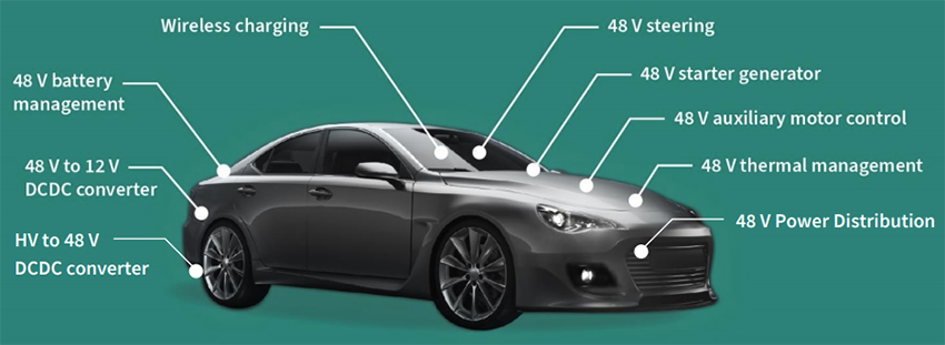
These Infineon MOSFETs are optimized for 48V automotive systems and are widely used in applications such as DC‑DC converters, motor control for pumps/fans, power distribution, and battery management systems. The devices also enable critical functions in electric power steering, braking, LED lighting, and light electric vehicle subsystems, where efficient power conversion and robust switching are essential. Overall, the OptiMOS 7 100V family supports the transition to more electrified, energy-efficient vehicles by improving system performance while simplifying thermal and space constraints.
Features
- OptiMOS power MOSFET for automotive applications
- N‑channel, enhancement mode
- Logic level for IAUCN10S7L290T
- Normal level for IAUCN10S7N025T
- Extended qualification beyond AEC‑Q101
- Enhanced electrical testing
- Minimized conduction losses
- Superior switching performance
- High power density and efficiency
- Increased current capability
- Very low RDS(on)
- Robust design
- PG‑LHDSO‑10 package
- Moisture Sensitivity Level (MSL) 1 up to +260°C peak reflow
- -55°C +175°C operating temperature range
- 100% avalanche tested
- RoHS compliant
Applications
- DC-DC converters (power conversion)
- Motor control systems
- Automotive auxiliary loads
- Power distribution and switching
- Battery Management Systems (BMS)
- Steering and safety systems
- Lighting systems
- Electric and light mobility platforms
Specifications
- Static characteristics
- 100V minimum drain‑source breakdown voltage
- 1.2V to 3.2V gate threshold voltage range
- 1μA to 29μA zero gate voltage drain current range
- 100nA maximum gate-source leakage current
- 2.5mΩ to 38.2mΩ drain‑source on‑state resistance
- 0.9Ω to 1.5Ω typical gate resistance range
- Dynamic characteristics
- 560pF to 6600pF maximum input capacitance range
- 240pF to 2760pF maximum output capacitance range
- 8pF to 30pF maximum reverse transfer capacitance range
- 2ns to 16ns typical turn-on delay time range
- 2ns to 15ns typical rise time range
- 8ns to 33ns typical turn-off delay time range
- 4ns to 18ns typical fall time range
- Gate charge characteristics
- 1.8nC to 31nC maximum gate-to-source charge range
- 3nC to 19nC maximum gate-to-drain charge range
- 11nC to 93nC maximum gate charge total range
- 3.1V to 4.6V typical gate plateau voltage range
- Reverse diode characteristics
- 27A to 175A maximum diode continuous forward current range
- 52A to 622A maximum diode pulse current range
- 1V maximum diode forward voltage
- 32ns to 68ns maximum reverse recovery time range
- 15nC to 82nC maximum reverse recovery charge range
- Single pulse avalanche
- 12mJ to 139mJ maximum energy range
- 18A to 125A maximum current range
- 45W to 205W maximum power dissipation range
Datasheets
Schematic

OptiMOS™ 7 Automotive Power MOSFETs

Infineon Technologies OptiMOS™7 Automotive Power MOSFETs
Implements Power MOSFET technology with 40V innovative, leadless, robust power packages.
Infineon Technologies OptiMOS™ 7 80V Automotive Power MOSFETs
Designed for high-performance, quality, and robustness needed for demanding automotive applications.

Infineon Technologies OptiMOS™ 7 40V Automotive Power MOSFETs
Offer high power density, low conduction losses, and optimized switching behavior.