









Abracon ABFBxx Clock Buffers

Abracon ABFBxx Clock Buffers distribute precision clock signals to multiple low-jitter outputs for PCIe, networking, telecom, computing, and industrial timing applications. The portfolio includes PCIe, differential, and CMOS fanout buffers with support for HCSL, LVPECL, LVDS, and LVCMOS interfaces. These features give designers flexible clock distribution options across high-speed systems.
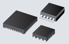
The Abracon ABFBxx Clock Buffers include the 20-output ABFB20HA2A PCIe buffer, 10-output ABFB10XC3A differential buffer, 10-output ABFB10CB1A LVCMOS buffer, and 4-output ABFB04XB1A differential buffer. The devices combine femtosecond-level additive jitter, low output skew, industrial temperature operation, and compact VQFN or WGQFN package options. The devices support PCIe Gen 5/6 clock distribution, low-jitter clock trees, logic translation, wired and wireless communications, server platforms, storage systems, switches, routers, and test equipment.
Features
- Fanout buffer for distributing precision clock signals to multiple low-jitter outputs
- PCIe fanout buffer support for PCIe Gen 1 through Gen 6 and Intel QPI clock distribution
- Differential fanout buffer options with LVPECL, LVDS, HCSL, and LVCMOS output support
- CMOS fanout buffer option with independently selectable LVCMOS output voltage support
- 3-to-1 input multiplexer options accepting differential, single-ended, or crystal inputs
- Embedded LDO voltage regulator on ABFB20H, ABFB10X, and ABFB04X devices for improved power supply noise rejection
- SMBus and Side-Band Interface support on ABFB20HA2A for flexible PCIe clock buffer control
- Control pin-based configuration on ABFB10XC3A, ABFB10CB1A, and ABFB04XB1A devices
- REACH/RoHS II compliant construction with MSL Level 3 rating
Applications
- PCIe Gen 1 through Gen 6 clock distribution
- Low-jitter clock trees
- Logic translation
- Clock and data signal restoration
- Wired communications, including OTN, SONET/SDH, GE, 10GE, FC, and 10G FC
- Wireless communications
- High-performance microprocessor clock distribution
- Servers, storage, and data centers
- Switches and routers
- Test equipment
Specifications
- ABFB04XB1A
- Four differential LVPECL/LVDS/HCSL outputs and one LVCMOS output
- Frequency range of 0MHz to 1.6GHz
- Additive jitter of 24fs at 625MHz from 12kHz to 20MHz
- Maximum output-to-output skew of 40ps
- LVPECL/LVDS/HCSL output supply of 2.5V or 3.3V
- LVCMOS output supply of 1.5V, 1.8V, 2.5V, or 3.3V
- 32-pin VQFN package, 5mm x 5mm x 0.9mm
- Operating temperature range of -40°C to +85°C
- ABFB10CB1A
- 10 LVCMOS outputs
- Frequency range of 0MHz to 200MHz
- Crystal support from 8MHz to 60MHz
- Additive jitter of 17fs from 12kHz to 20MHz
- Ultra-low noise floor of -170dBc/Hz
- Typical output-to-output skew of 30ps
- Typical input-to-output delay of 2ns
- LVCMOS output supply of 1.5V, 1.8V, 2.5V, or 3.3V
- 32-pin VQFN package, 5mm x 5mm x 0.9mm
- Operating temperature range of -40°C to +85°C
- ABFB20HA2A
- 20 low-power HCSL PCIe outputs
- Fully compliant with the Intel DB2000QL specification
- PCIe Gen 5.0 and Gen 6.0 support
- Frequency range of 0MHz to 250MHz
- Additive jitter of 14fs typical in the DB2000QL band
- Maximum output-to-output skew of 50ps
- 3.3V supply voltage
- 80-pin WGQFN package, 6.0mm x 6.0mm x 0.75mm
- Operating temperature range of -40°C to +85°C
- ABFB10XC3A
- 10 differential LVPECL/LVDS/HCSL outputs and one LVCMOS output
- Frequency range of 0MHz to 1.6GHz
- Additive jitter of 24fs at 625MHz from 12kHz to 20MHz
- Maximum output-to-output skew of 40ps
- LVPECL/LVDS/HCSL output supply of 2.5V or 3.3V
- LVCMOS output supply of 1.5V, 1.8V, 2.5V, or 3.3V
- 48-pin VQFN package, 7mm x 7mm x 0.9mm
- Operating temperature range of -40°C to +85°C
Additional Resources
ABFB20HA2A Functional Block Diagram

ABFB10XC3A Functional Block Diagram

ABFB10CB1A Functional Block Diagram

ABFB04XB1A Functional Block Diagram
